

IGBT damage frequently starts with energy stored in the busbar, module, transformer, and PCB inductance. During the turn-off, that energy produces a voltage overshoot. A proper RCD Snubber Capacitor absorbs the transient. The resistor and diode control its release. The best choice matches the measured waveform. It also fits the mounting loop and temperature.
Check the highest turn-off current. Look at unsuppressed voltage overshoot, ringing frequency, and estimated parasitic inductance. Selecting a capacitor only from the nominal DC-bus voltage can leave it unable to handle the energy. This energy appears during a fast switching event.
The energy comes from more than the IGBT itself. Long laminated busbars, transformer leakage, connector paths, and module terminals can all add inductance. Engineers should therefore measure the actual switching node. They should not depend entirely on a schematic-based estimate.
Voltage rating is only the first filter. Pulse-current capability determines whether the capacitor can accept the transient repeatedly. ESR affects internal heating. ESL is just as important. The capacitor must respond before the voltage spike reaches a dangerous level.
The selected RCD Snubber Capacitor should also tolerate the system's dV/dt and peak current. A component with adequate voltage but excessive inductance may reduce later ringing. It may still fail to control the first and most damaging overshoot.
Higher switching frequency increases the number of charge-and-discharge cycles per second. This raises average dissipation. Elevated temperature reduces voltage margin. It may shorten service life. Package layout changes the total inductance added by terminals, leads, and mounting hardware.
A smaller capacitor positioned directly beside the IGBT may work better than a physically larger unit. The larger unit connects through long conductors. This is why electrical sizing and mechanical layout should be evaluated together.
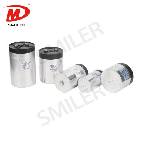
Direct-mount film capacitors suit industrial motor drives, high-current inverters, welding power supplies, and other equipment with large IGBT modules. Their main advantage is the ability to minimize the transient-current loop. This loop forms between the switching device and the snubber network.
SMILER capacitor MKPH-S is designed for IGBT buffer circuits. It provides several terminal and installation arrangements. Its metallized polypropylene construction supports high pulse intensity, self-healing behavior, flame resistance, and repeated switching stress. The series is available across a broad voltage and capacitance range. This allows it to serve different module sizes without forcing a long connection path.
Leaded capacitors are useful when rigid module terminals are impractical. They are also useful when the snubber must fit into a crowded PCB assembly. They offer more installation flexibility. They must be placed carefully because excessive lead length adds unwanted ESL.
SMILER capacitor DC Link MKP-LS uses metallized polypropylene film with tinned copper wire, copper plugs, or flexible leads. It is intended for IGBT surge absorption, peak-voltage clamping, inverter systems, frequency converters, and high-frequency resonant circuits. Its compact size and low ESR make it practical for designs where heat dissipation and board space must be balanced.
This option suits systems with high DC-bus voltage, sharp dV/dt, and relatively limited stored parasitic energy. The goal is to clamp the initial spike. It avoids adding unnecessary charge that must be moved during every switching cycle.
Priority should be given to voltage margin, pulse-current capability, dV/dt, and low inductance. Simply increasing capacitance can slow the waveform. It can raise peak snubber current and add switching loss. Fast-switching prototypes should therefore begin with a controlled value. They should increase it only when measurements show insufficient suppression.
Long busbars, high turn-off current, transformer leakage, or larger inverter assemblies may require greater capacitance. A higher-capacitance RCD Snubber Capacitor can absorb more transient energy. It reduces the voltage rise more effectively.
However, more capacitance is not automatically safer. The resistor must dissipate more energy. The diode may carry a larger pulse. The IGBT can experience increased switching loss. The value should be raised gradually. This is done while monitoring overshoot, ringing duration, capacitor temperature, and resistor heating.
Standard packages may not fit unusual busbar spacing, terminal direction, enclosure height, or insulation-clearance requirements. In these cases, a customized solution can reduce loop length more effectively. It works better than adapting a standard capacitor with extra brackets or wiring.
We support customized capacitance, voltage, dimensions, terminal forms, and installation arrangements. Customization should begin with actual mechanical drawings, operating voltage, switching frequency, current waveform, temperature range, and measured overshoot. Changing the enclosure alone is not enough. The internal electrical stress must also remain within limits.
Measure the DC-bus voltage, peak collector-emitter voltage, turn-off current, ringing frequency, and waveform duration under the worst expected load. Measurements should cover startup, full load, regenerative conditions, and maximum line voltage.
A short probe connection is essential. A long ground lead can create artificial ringing. This makes the overshoot appear worse than it is. Whenever possible, use a differential probe, spring ground, or coaxial measurement method.
Use parasitic energy and the permitted clamp-voltage rise to establish a starting value. Real circuit inductance rarely matches a simplified estimate. Prototype tuning remains necessary.
The resistor must discharge the capacitor before the next switching event. It must do so without overheating. The diode needs adequate reverse voltage, peak current, and recovery speed.
Verify repetitive pulses at maximum line, load, frequency, and temperature. Include component tolerance and hotspot temperature. Do not rely on a single room-temperature test.
Place the capacitor and diode beside the IGBT switching terminals. The loop should have a minimum area. It should use wide, short conductors. A distant snubber may absorb later oscillations. It may respond too slowly to the first voltage peak.
Direct-terminal mounting normally provides the lowest loop inductance. Busbar mounting supports high current and mechanical stability. Leaded mounting offers flexibility for compact boards.
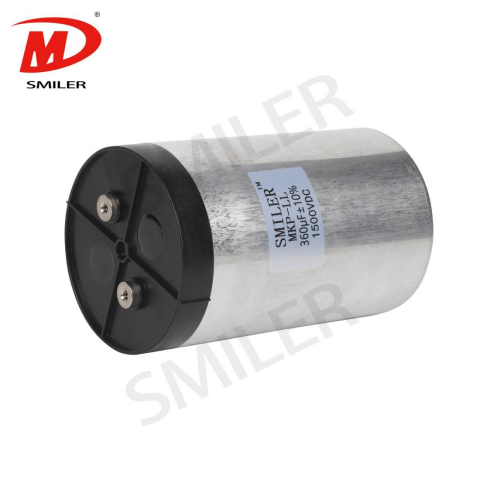
Snubbing must also be separated from bulk energy storage. Our DC Link MKP-LL is designed for DC-link circuits. It offers low ESR, high ripple current, and long operating life. It supports the inverter's bus voltage. MKPH-S snubber capacitor or MKPH-LS products address local IGBT switching transients.
Repeat the test with a spring ground, differential probe, or coaxial connection. Large waveform changes after moving the probe often indicate measurement-loop inductance.
Record peak voltage, ringing amplitude, ringing duration, switching energy, and waveform repeatability. A lower spike is not sufficient evidence of a better design. This is true if the turn-off loss or snubber dissipation rises excessively.
Test maximum DC-bus voltage, peak load current, startup, shutdown, regenerative operation, highest switching frequency, and elevated enclosure temperature. Repeated pulse testing is more representative than a single switching event.
Take thermal measurements after steady operation. A stable waveform can still hide an overloaded resistor, a slow diode, or an overheating capacitor.
A: Start with measured overshoot, turn-off current, switching frequency, temperature, and mounting distance. Then compare voltage, dV/dt, pulse current, ESR, ESL, capacitance tolerance, and package geometry.
A: It should absorb enough parasitic energy to keep the IGBT below its safe voltage limit. It must avoid creating excessive current or switching loss. Begin with an estimated value and tune it through controlled prototype testing.
A: Install it as close as possible to the IGBT switching terminals. The shortest practical path through the capacitor, diode, and resistor normally provides the fastest and most effective suppression.
A: It can. Excessive capacitance, an unsuitable resistor, or poor discharge timing increases current and heat. Proper sizing balances voltage suppression, resistor dissipation, diode stress, and IGBT switching energy.
A: Compare unsnubbed and snubbed waveforms at maximum line, load, frequency, and temperature. Confirm peak voltage, ringing, switching loss, resistor temperature, diode behavior, and capacitor temperature during extended operation.
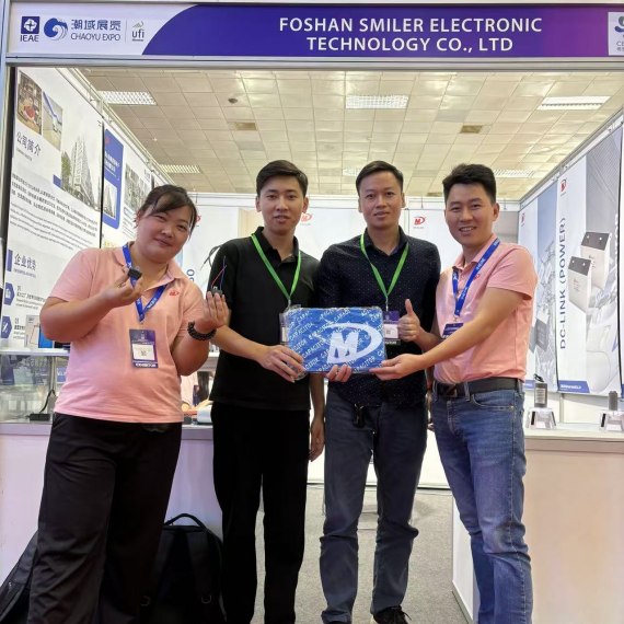
2024 VIETNAM INTERNATIONAL ELECTRONICS & SMART APPLIANCES EXPO
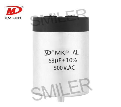
Exploring How AC Capacitors and DC Capacitors Function Differently
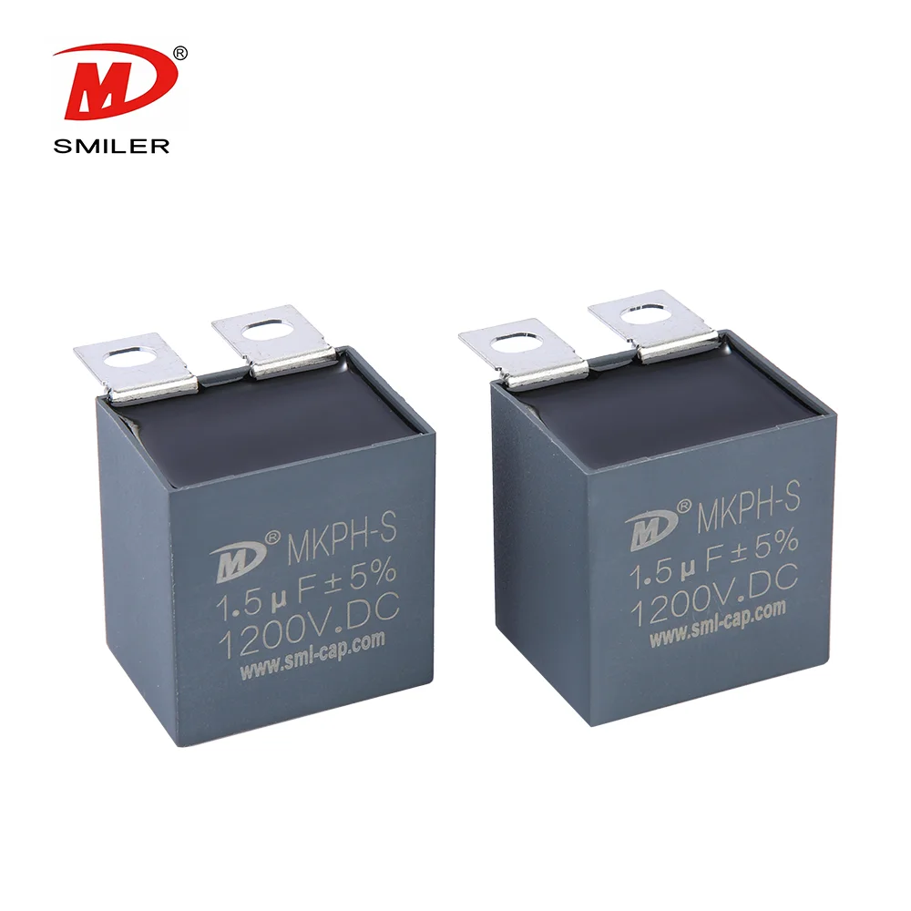
Understanding Snubber Capacitor: RC vs. RCD Snubber Differences
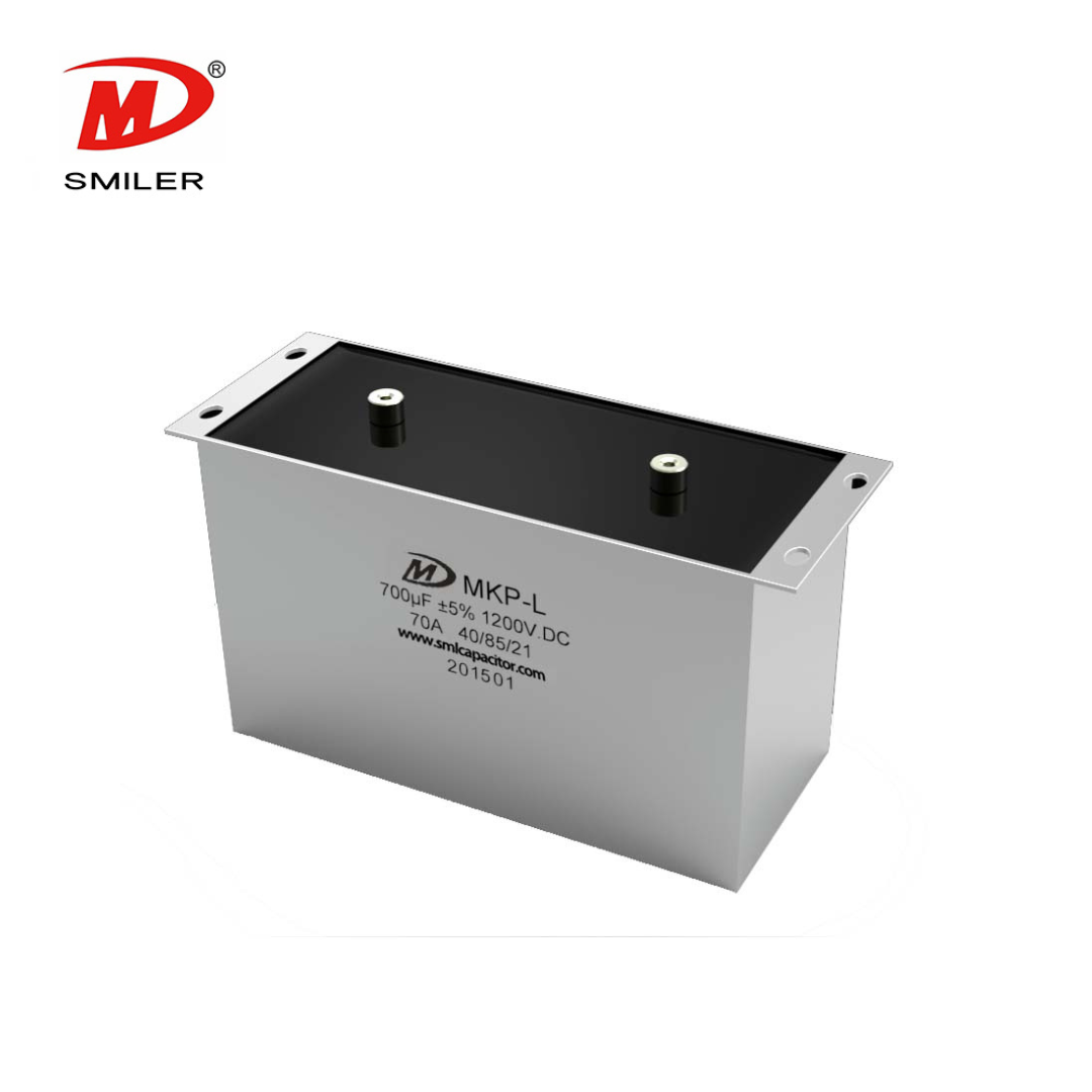
Understanding DC Capacitance to Prevent Converter Oscillations
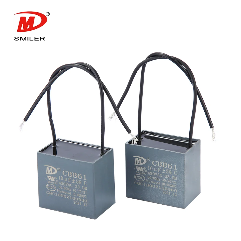
What Does a CBB61 Fan Capacitor Do? Exploring the Role of CBB61 Fan Capacitors


 Add
Building 12,Huazhi Technology Innovation Center,28 Sanle East Road,Beijiao,Foshan,Guangdong,China
Add
Building 12,Huazhi Technology Innovation Center,28 Sanle East Road,Beijiao,Foshan,Guangdong,China
 Phone
+86 18007576965 / 0757-22391591
Phone
+86 18007576965 / 0757-22391591
 Email
ari@sml-cap.cn
Email
ari@sml-cap.cn



