

Electromagnetic interference becomes harder to control as switching edges accelerate and PCB layouts grow denser. A conventional bypass capacitor may provide enough attenuation at modest frequencies, yet its leads, pads, and ground connection add inductance that limits performance in the upper-frequency range. A 3 terminal filter capacitor addresses that weakness with a feed-through current path and a dedicated, low-inductance connection to ground.
In a standard bypass arrangement, current travels along a trace while a two-terminal capacitor branches from that trace to ground. The branch adds pad, trace, and via inductance. A feed-through device instead makes the power or signal conductor enter one line terminal and leave through the other. High-frequency noise is diverted through the ground electrode at the component, so the filtering path is part of the main current route rather than a side branch. This distinction is central to capacitor filter circuit fundamentals.
The name describes three electrical nodes, not necessarily three visible pads. Many surface-mount versions use two line electrodes connected internally as one feed-through conductor, plus two ground electrodes connected to the same ground node. The duplicated ground pads create short, symmetrical return paths and make a compact four-pad footprint possible. Engineers should therefore confirm the manufacturer’s terminal diagram instead of counting pads. Reversing a line and ground connection can defeat filtering or create an unintended short circuit.
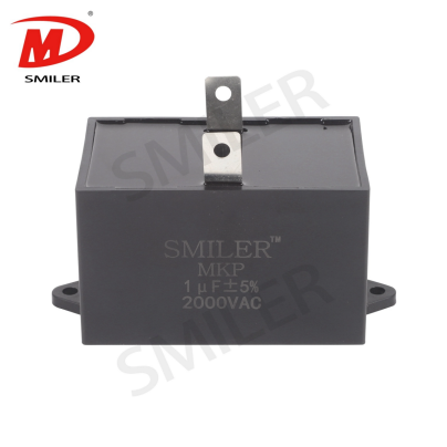
Every real capacitor contains equivalent series resistance and equivalent series inductance, or ESL. Capacitance controls the falling impedance region, while ESL eventually makes impedance rise again. The feed-through geometry reduces the inductive portion of the current loop, pushing the useful low-impedance range to a higher frequency and supporting broader insertion loss. It does not eliminate self-resonance; it makes parasitic inductance less dominant. The interaction is easier to interpret alongside ESR and low-pass filter performance.
Noise attenuation depends on the impedance of the complete loop, not the capacitor value alone. A long ground trace or distant via contributes inductive reactance that rises with frequency. Placing ground pads directly over a solid reference plane and using nearby vias minimizes this shared path. The capacitor can then shunt common high-frequency energy before it spreads across the board. Several small vias often produce lower effective inductance than one remote via, provided the layout maintains a short and uninterrupted return path.
A two-terminal multilayer ceramic capacitor can show low impedance in a bench fixture yet deliver less attenuation after PCB interconnect inductance is added. A 3 terminal filter capacitor is evaluated as a feed-through network, so insertion loss is usually the more useful comparison. Its curve can remain effective over a broader high-frequency band because input, output, and ground paths are controlled. Engineers should compare data measured with similar source impedance, load impedance, mounting pattern, DC bias, and temperature; otherwise, attractive curves may not predict circuit behavior.
Sometimes it can replace multiple parallel bypass capacitors used only to cover adjacent high-frequency bands. The compact device may also reduce routing area and the number of ground stubs. However, it is not automatically equivalent to an LC or pi filter. Inductors provide series impedance, while a feed-through capacitor primarily offers a low-impedance shunt. Required attenuation, current, transient energy, source stability, and load behavior must be reviewed before parts are removed. Prototype measurements should decide whether consolidation is safe.
The trace should enter the input pad and continue from the output pad without a parallel bypass around the package. This forces unwanted high-frequency current to encounter the intended filtering structure. Placement close to the noise source prevents the unfiltered trace from acting as an antenna, while placement near a connector can stop noise from leaving the board. The better location depends on whether the goal is source containment or interface protection. In both cases, minimize copper length on the noisy side.
Common errors include connecting the ground electrodes through a thin neck, sharing a long return with switching current, placing vias far from the pads, and crossing a split in the reference plane. These features increase loop area and common impedance. Another mistake is routing input and output traces close together, which allows capacitive or magnetic coupling around the filter. Keep the two sides physically separated, preserve a continuous ground plane, and follow the tested land pattern whenever measurement repeatability matters.
Capacitance is only the starting point. Selection should also cover:
*Rated voltage, DC-bias behavior, and dielectric temperature characteristics.
*Current capability, DC resistance, temperature rise, and allowable ripple.
*Insertion loss across the actual noise band, plus package and land-pattern limits.
The source and load impedances used for published data may differ sharply from a powered circuit. At SMILER capacitor, we distinguish PCB-level feed-through filtering from other capacitor duties so engineers do not treat unrelated component categories as interchangeable. Final selection still requires application-specific electrical and thermal review.
Start with a repeatable baseline using the same board, cables, operating state, enclosure, and instrument settings. For conducted noise, compare spectra with a suitable line impedance stabilization network or controlled test fixture. For radiated noise, control cable position and antenna distance. Near-field probes can locate local changes but do not replace compliance testing. Record noise amplitude across the problem band, component temperature, and any new resonance. An A/B board with only the filter population changed gives more reliable evidence than comparing unrelated prototypes.
The device is useful where a trace carries required low-frequency or DC energy while unwanted high-frequency content must be sent to ground. Typical candidates include clocked digital supply branches, sensor rails, compact converter control boards, and noisy lines approaching an external connector. It is especially attractive when conventional bypass performance is limited by mounting inductance. Signal integrity must still be checked on fast data lines because excessive capacitance can slow edges, increase jitter, or load the transmitter.
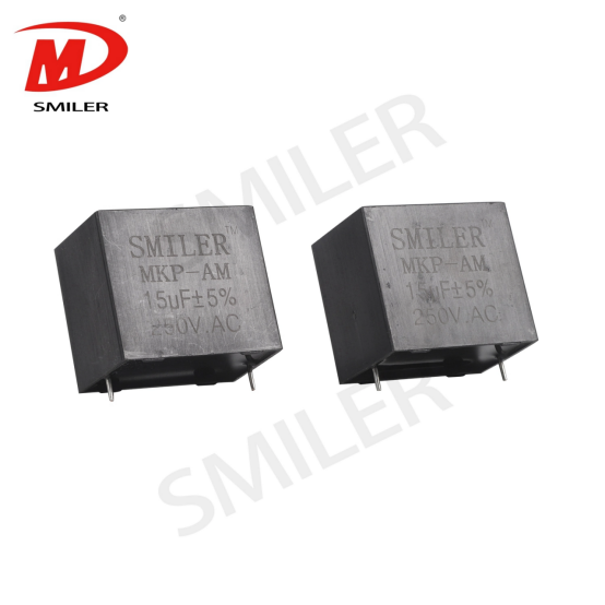
A two-terminal capacitor remains practical when frequencies are moderate, space is available for a very short ground connection, or cost dominates. LC and pi networks are better when strong series impedance is required, while RC or RCD snubbers target ringing at a switching node. High-energy AC filtering is another distinct duty. For example, our MKP-AM AC filter capacitor uses metallized polypropylene film for converter output filtering; it is not a 3 terminal feed-through capacitor. Match the topology to the noise source, energy level, and safety requirements.
A: It passes the required current through two line connections while shunting high-frequency noise through a dedicated ground node. The arrangement is used to improve EMI attenuation when the inductance of a conventional bypass connection would otherwise limit performance.
A: Its feed-through structure integrates the line path and places the ground connection close to the internal electrodes. That geometry shortens the high-frequency loop and reduces mounting inductance, although the actual result still depends on pads, vias, and the reference plane.
A: It can replace a two-terminal bypass capacitor when broader high-frequency attenuation and a controlled feed-through path are needed. It should not be treated as a universal drop-in replacement because its footprint, current path, grounding, voltage rating, and signal loading differ.
A: Place it so the noisy trace passes through the line terminals and the ground electrodes connect to a continuous plane with very short paths. Position it close to the noise source for containment or near an interface when preventing cable-borne emissions is the priority.
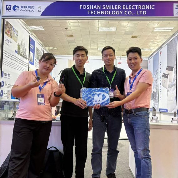
2024 VIETNAM INTERNATIONAL ELECTRONICS & SMART APPLIANCES EXPO
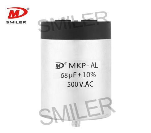
Exploring How AC Capacitors and DC Capacitors Function Differently
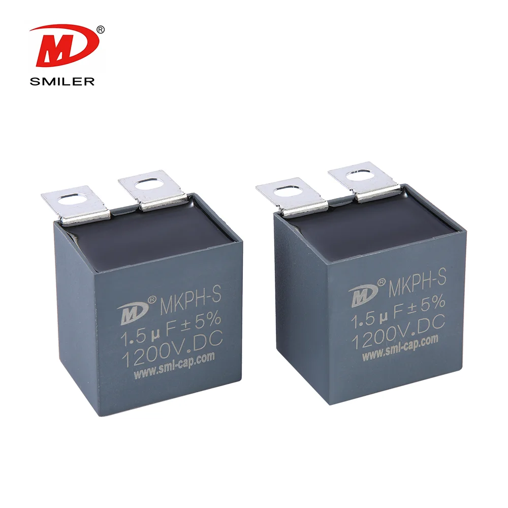
Understanding Snubber Capacitor: RC vs. RCD Snubber Differences
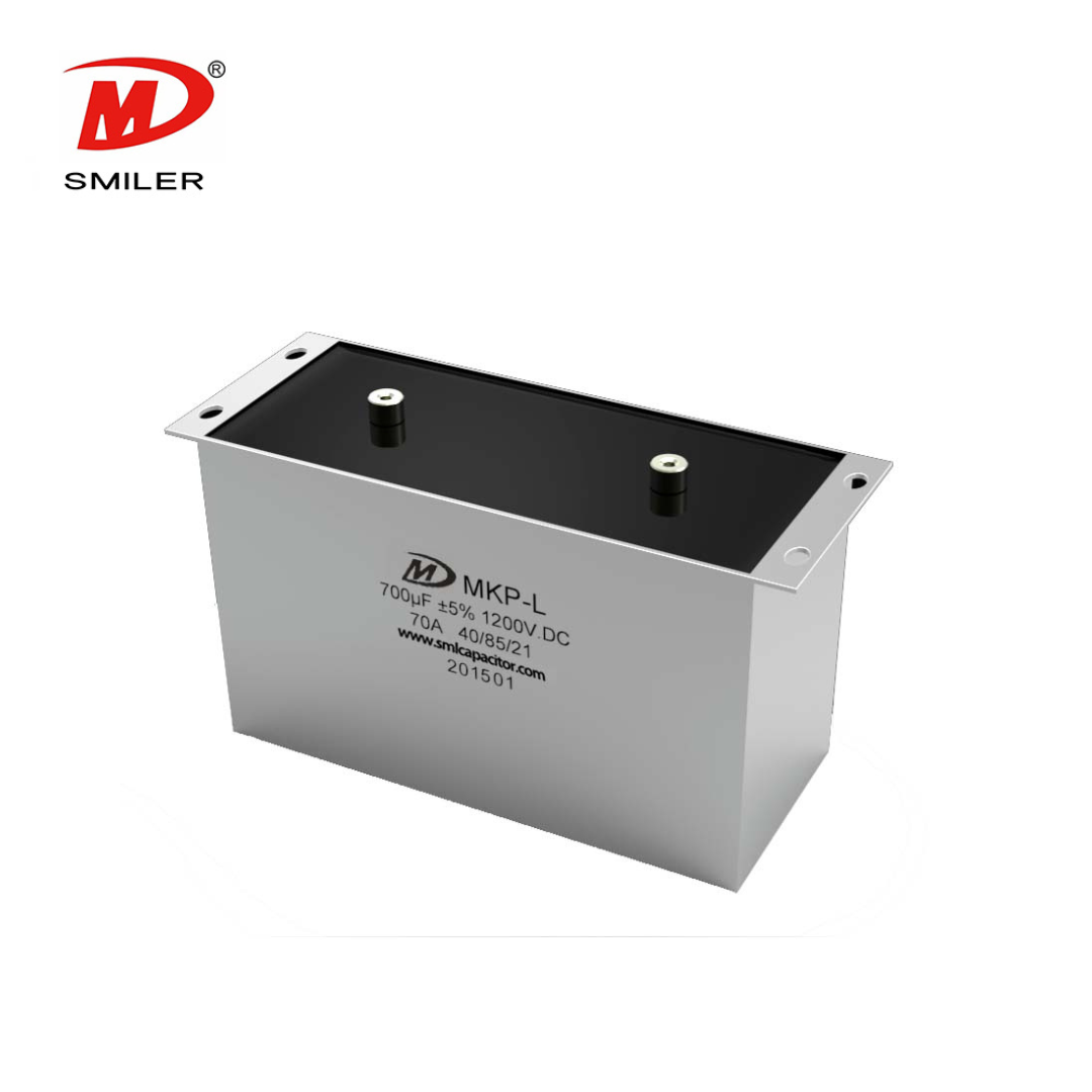
Understanding DC Capacitance to Prevent Converter Oscillations
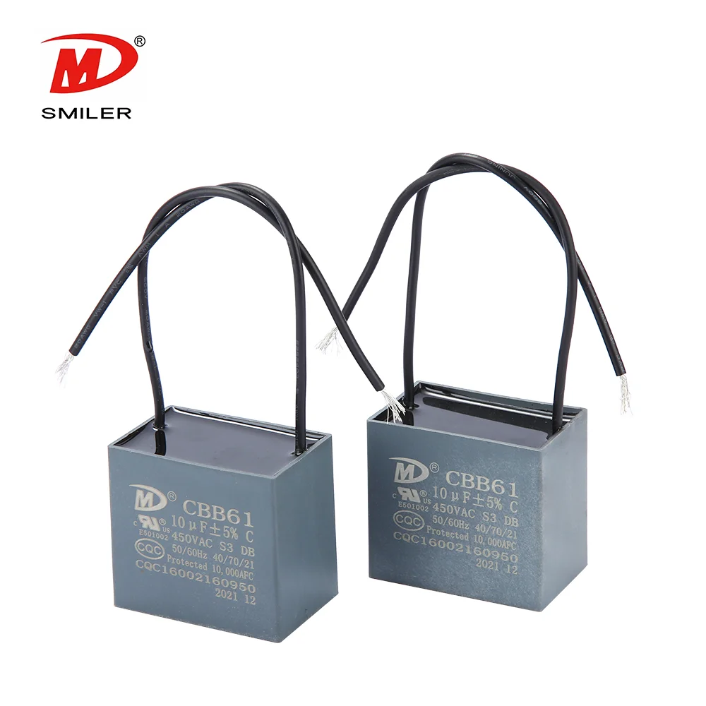
What Does a CBB61 Fan Capacitor Do? Exploring the Role of CBB61 Fan Capacitors


 Add
Building 12,Huazhi Technology Innovation Center,28 Sanle East Road,Beijiao,Foshan,Guangdong,China
Add
Building 12,Huazhi Technology Innovation Center,28 Sanle East Road,Beijiao,Foshan,Guangdong,China
 Phone
+86 18007576965 / 0757-22391591
Phone
+86 18007576965 / 0757-22391591
 Email
ari@sml-cap.cn
Email
ari@sml-cap.cn



