

The DC bus may look steady, yet an oscilloscope can reveal a sharp overshoot whenever a MOSFET or IGBT switches. Adding bulk capacitance after the rectifier can reduce low-frequency ripple, but it may do little to stop fast ringing. A snubber capacitor addresses a different problem: it gives transient current a short, controlled path, limiting the voltage rise at its source instead of merely storing more energy on the DC bus.
Device leads, PCB traces, busbars, transformer leakage, and package connections all store magnetic energy. When a switch turns off quickly, current cannot stop instantly. The practical relationship V = L × di/dt explains why even small parasitic inductance can produce a large spike at high di/dt.
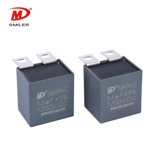
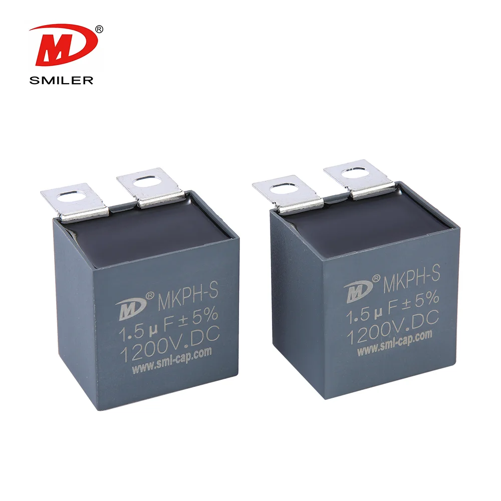
A snubber capacitor receives commutation current that would otherwise force the switch voltage upward. In an RC network, the resistor converts captured energy into heat and damps the parasitic LC oscillation. SMILER capacitor supplies dedicated snubber products for this switching-stage duty. Our Power Capacitor Snubber Capacitor MKPH-S is intended for IGBT snubbering and switch-mode power supplies, a different function from reservoir or DC-link capacitance.
Repeated overshoot consumes voltage margin and stresses semiconductors. Ringing can cause false triggering, unstable gate drive, EMI, insulation stress, and local heating. Equipment may pass bench tests yet age faster in service.
A capacitor-only snubber slows dv/dt and reduces peak voltage. It adds no resistive damping, so energy may keep oscillating. Stored charge also produces extra turn-on current. Use it only when the circuit provides enough damping.
The capacitor diverts transient current; the resistor controls how its energy dissipates. Together they reduce the Q of the parasitic LC network, lowering overshoot and ringing. The resistor must handle repetitive power, and the capacitor must tolerate pulse current and rapid voltage change.
An RCD snubber separates charging and discharging with a diode. It responds mainly during the harmful transition while the resistor resets the capacitor. Compare an RCD snubber capacitor and an RC snubber against loss, thermal limits, and switching direction.
No. A reservoir capacitor reduces rectified ripple, while a DC-link capacitor supports the intermediate bus. A snubber manages fast transients close to a switch, diode, or power module. Similar-looking parts are not interchangeable because their stress and placement differ.
In commercial energy-storage inverters, the documented component map assigns the MKP-LM Series to DC filtering and smoothing, a dedicated snubber to IGBT protection, and the MKP-AM Series to output filtering. Distributed solar inverters use the same three functional stages. That division illustrates why location after rectification alone does not define a capacitor's job.
Those commercial and distributed-solar maps list MKP-LM at 1–170 μF and 450–1200 Vdc, while MKP-AM covers 0.47–50 μF and 160–450 Vac.
Reverse recovery changes diode current abruptly. Leakage and wiring inductance interact with stray capacitance, producing ringing. An RC network can sit across the affected diode, winding, or switching node in a short loop.
The functional path is:
Rectifier → smoothing or DC-link stage → switching bridge or converter.
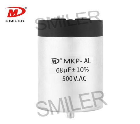
The snubber belongs beside the MOSFET, IGBT, diode, or module producing the transient—not at an arbitrary point on the rectified bus. In central solar converters, the documented component map assigns the MKP-LL Series to DC-link filtering and smoothing, the MKPH-S Series to IGBT snubber protection, and the MKP-AL Series to output filtering. Wind-power converters repeat those three roles with the same three series.
Medium- and high-voltage drives separate an MKP-LL Series DC-link capacitor for filtering and smoothing from an MKPH-S Series snubber for IGBT protection. SVC and SVG equipment use that same two-part assignment. Fast-charging systems likewise pair MKP-LL Series DC-link filtering and smoothing with MKPH-S Series snubber and IGBT protection. These examples place energy buffering and transient control in separate components.
For central solar applications, that map lists the MKPH-S snubber at 0.1–4.0 μF and 850–2000 Vdc, alongside an MKP-LL DC-link range of 170–2200 μF at 600–1500 Vdc and an MKP-AL output-filter range of 3 × 8 μF to 3 × 335 μF at 230–850 Vac.
Measure ringing frequency, peak overshoot, switched current, bus voltage, switching frequency, and operating extremes. Use a high-bandwidth probe with a short ground connection; a long probe loop can display measurement-induced ringing.
Begin with parasitic energy: E = 0.5 × Lp × I². For allowed rise ΔV, capacitor energy is E = 0.5 × Csnub × (ΔV)². Equating them gives an initial value because real paths contain other capacitances and losses.
A practical damping estimate is:
Rsnub ≈ √(Lp/Cp)
Lp and Cp represent effective parasitic inductance and capacitance. Adjust R and C while observing overshoot, decay, resistor temperature, and switching loss.
Rate the part for repetitive transients, checking peak and RMS current, dv/dt, pulse repetition, and temperature. The snubber belongs beside a separately assigned DC-link capacitor rather than treating one device as both.
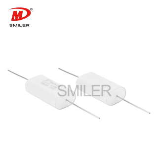
Low ESL helps intercept a fast edge; ESR affects heating and damping. The compact Power Capacitor Snubber Capacitor MKPH-LS uses metallized polypropylene and is specified for low self-inductance, low ESR, IGBT surge absorption, and high-frequency resonant circuits. Confirm temperature stability, the measured waveform, and mounting geometry.
Connection inductance can isolate a correctly calculated snubber. Keep the loop short and wide, place components beside the protected device, and keep transient current out of shared control or gate-return paths.
Too little capacitance leaves overshoot or ringing. Too much raises current, heat, and switching loss, and may only move the resonance.
Test high and low input voltage, load extremes, startup, regeneration, temperature, and tolerances. A value tuned at one point can fail as current, inductance, or switching speed changes. Confirm semiconductor margin and snubber temperature.
A: Only if its construction, ratings, and placement suit the transient. A bulk capacitor after a rectifier usually smooths low-frequency ripple. A snubber capacitor must handle repetitive pulse current and sit close to the device or node producing the spike.
A: Place it at the transient source, such as the rectifier diode, MOSFET, IGBT, transformer winding, or power module. Keep the loop short and wide. DC-bus position alone does not make the connection effective by itself.
A: A DC-link capacitor buffers energy and stabilizes the intermediate bus. A snubber capacitor controls fast overshoot and ringing at a switching node. Their capacitance, pulse-current stress, parasitic inductance, and physical placement are therefore selected for different tasks.
A: Fast current interruption interacts with transformer leakage, wiring, package, and PCB inductance. Diode reverse recovery can intensify the event. The resulting parasitic LC network produces overshoot and ringing that ordinary bulk capacitance may not suppress.
A: Measure ringing frequency, overshoot, switched current, bus voltage, and operating extremes. Estimate C and R, then tune on the real waveform. Verify voltage, dv/dt, pulse current, ESR, ESL, temperature, resistor loss, and physical loop length.
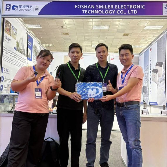
2024 VIETNAM INTERNATIONAL ELECTRONICS & SMART APPLIANCES EXPO
Exploring How AC Capacitors and DC Capacitors Function Differently
Understanding Snubber Capacitor: RC vs. RCD Snubber Differences
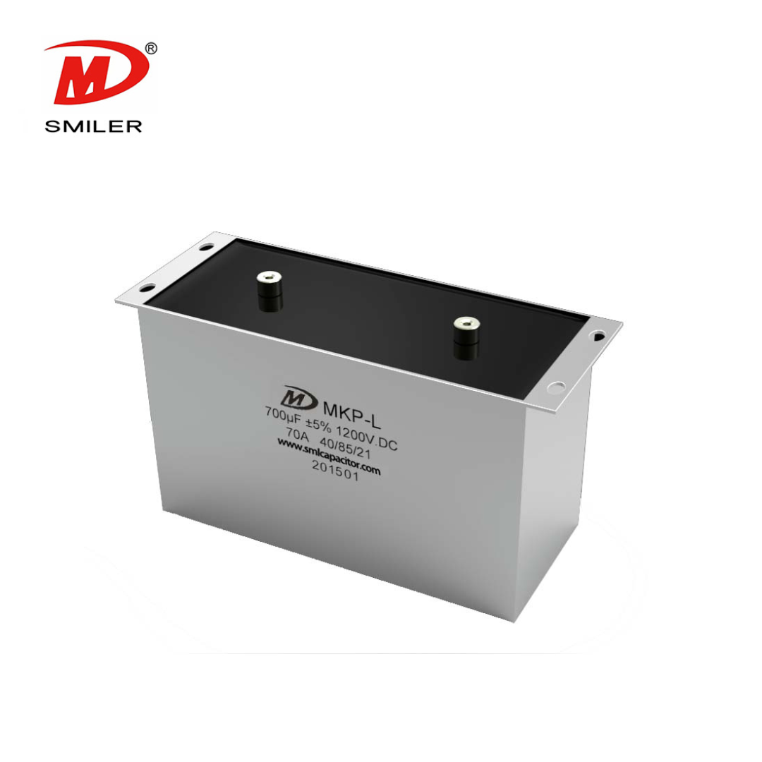
Understanding DC Capacitance to Prevent Converter Oscillations
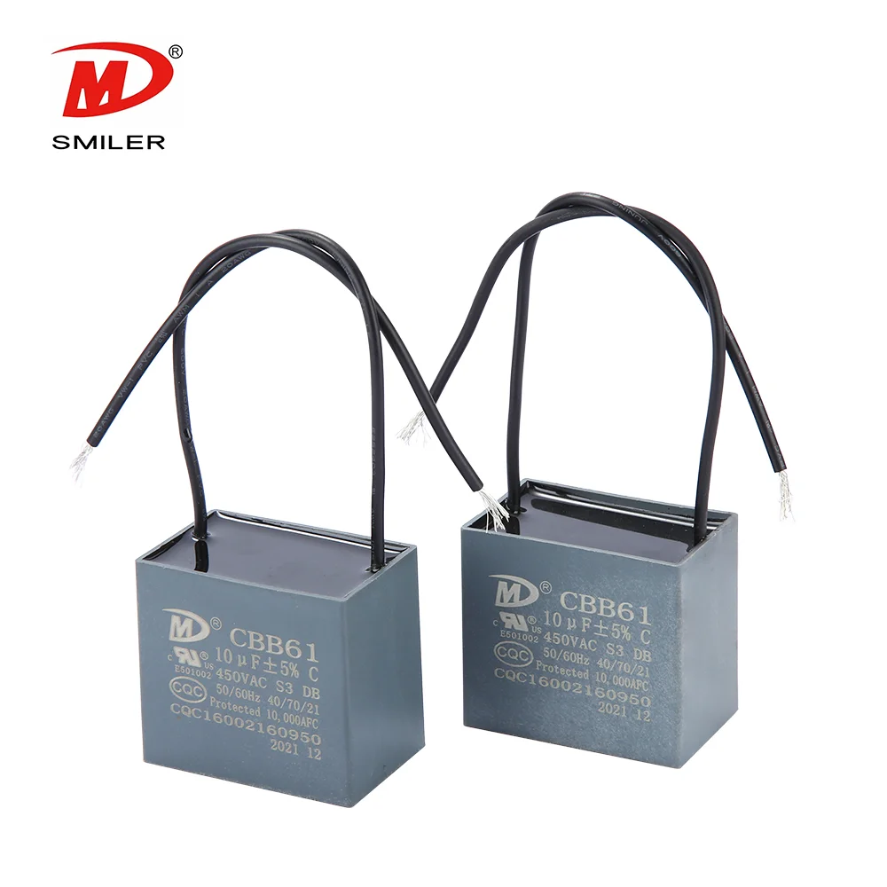
What Does a CBB61 Fan Capacitor Do? Exploring the Role of CBB61 Fan Capacitors


 Add
Building 12,Huazhi Technology Innovation Center,28 Sanle East Road,Beijiao,Foshan,Guangdong,China
Add
Building 12,Huazhi Technology Innovation Center,28 Sanle East Road,Beijiao,Foshan,Guangdong,China
 Phone
+86 18007576965 / 0757-22391591
Phone
+86 18007576965 / 0757-22391591
 Email
ari@sml-cap.cn
Email
ari@sml-cap.cn



